
Martin Pospíšilík
Faculty of Applied Informatics
Tomas Bata University
in Zlin
pospisilik@fai.utb.cz
AbstractThere are several applications in which a buttonless keyboard might be useful. In exteriors, they can capitalize on the fact that without buttons the keyboard can be fully closed and therefore it is weather resistant. Moreover, they seem to be easily made in vandalism resistant forms. Their considerable advantage also lies in the fact that they can be made in various design conceptions. Usually, several approaches to the buttonless keyboards are practiced. In this paper a design of a simple optical-based keyboard is described.
Klávesnice bez mechanických tlačítek mohou nalézt uplatnění v nemálo aplikacích. V exteriérech těží z toho, že je lze jednoduše vyrobit ve zcela uzavřeném provedení, a tím pádem odolné proti vlivům počasí, případně i vandalismu. Vneposlední řadě je lze vyrábět vrůzných designových provedeních. Voblasti této konstrukce tlačítek existuje nemálo přístupů, přičemž vtomto článku je popsán návrh jednoduché a snadno sestrojitelné klávesnice, která pracuje na optickém principu.
KeywordsOptical button, Photo sensor, Keyboard, Time division multiplex
Optotlačítka, optosenzor, klávesnice, časový multiplex
IntroductionThe design of an optical buttonless keyboard is based on the principle of optical push buttons that is well described [1].
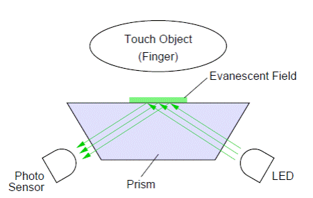
Fig. 1 – Basic conception of an optical push button [1]
The principle of operation of such optical push button is rather obvious. When a reflective object (a finger) moves close to the evanescent field, the light emitted by the LED is reflected into a photo sensor that drives the proper logical circuits. As stated in [1], this technology is rather new with only a few existing prototypes in this research field.
The main advantages of this solution are as follows:
The main disadvantages of this solution are as follows:
In order to prove the above mentioned theory a simple 4 button keyboard has been constructed. A great deal of effort was put into the following issues:
The solution is based on a time division multiplex. The keyboard consists of 4 couples of LEDs and a photo sensor. The working period of the keyboard consists of 4 timeslots. In each of them only one LED is driven and when the appropriate button is activated, the logical circuit detects that one the light of which is being reflected to the photo sensor. A block diagram of this solution is depicted in Fig. 2.
![]()
![]()
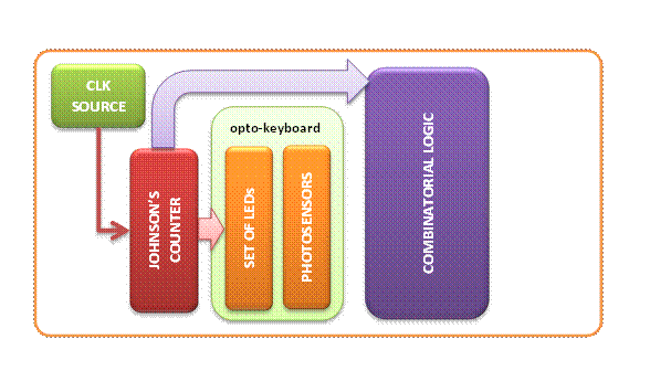
Fig. 2 – Buttonless optical keyboard test circuit block diagram
As can be seen in Fig. 2, the testing circuit can be divided into several blocks. The operating period is driven by a clock signal source. This source drives the Johnson’s counter that ensures sequential driving of appropriate LEDs. The reflections of the light emitted by the LEDs are captured by the photo sensors that are mounted close to the LEDs. The combinatorial logic then compares the waveforms of the signals that are present at the output of the Johnson’s counter and the output of the set of the photo sensors. When compliance between the signals is detected, the proper output of the output buffer is driven with a short logic signal. The output of the circuit can be then monitored by an oscilloscope or a multichannel logical probe.
Electrical designThe schema of the sample circuit that has been constructed and tested can be seen in Fig. 3.

Fig. 3 – Sample circuit schematic diagram
The sample circuit consists of three CMOS logical integrated circuits – Johnson’s counter IC1, quadruple NAND gate IC2 and sextuple NOT gate IC3. All three ICs are cheap and readily available.
The clock signal generator is made of IC3E and IC3F inverters. It runs with the frequency of approximately 1 kHz and drives the Johnsons’s counter IC1 whose number of possible states is restricted to 4 by connecting its Q4 output to its RESET input. Its outputs Q0 to Q3 are sequentially driven high, each for a period of approximately 250 µs. The prospective LEDs D1 to D4 glow when fed by the H level signal. The R15 resistor limits the current of the LEDs and ensures the appropriate level of the H signal at the outputs of IC1 which might fall below the IC2 threshold if the prospective outputs were loaded too much. The LEDs must therefore be capable of operation with low currents. Close to the LEDs complementary photo sensors are mounted. These photo sensors are based on phototransistors T1 to T4 with resistors R1 to R4 connected in their emitters. These resistors establish 100% negative feedback which decreases the sensitivity of the circuit to the ambient light. Normally, when no obstacle reflecting the light from the LEDs to the phototransistors is present, the phototransistors are variously opened which means that the voltage level at their emitters may vary according to the level of the ambient light. This does not affect the circuit operation as derivative members constructed with capacitors C1 to C4 and Zener diodes D10 to D13 are implemented in the circuit, making it insensitive to the non-fluctuating level of the ambient light. When a finger or any other reflective obstacle is enclosed, the ambient light is shielded with it and the light pulses generated by the prospective LED are reflected to the phototransistor. If the light pulses are sufficiently strong to cause current pulses of at least 0.5 mA sinking through the phototransistor, the prospective IC2 gate input is driven high. This high pulse occurs approximately at the same time (a small delay is tolerable) in which its second input is also driven high with the signal generated by IC1. This causes the gate output is turned to the low level, discharging the appropriate capacitor from the set of capacitors C5 to C8. The output of the relevant invertor IC3 is turned high for the time period in which the prospective capacitor is charged to the H level. This indicates the button has been hit.
The circuit is constructed to be supplied with the voltage of 5 V in order it could be employed together with microcontroller applications. The supply voltage is delivered through the SL1 connector and decoupled by the C10 capacitor. The IC1 and IC3 logical integrated circuits are supplied directly while the IC2 is supplied through the D9 diode. The voltage drop at the diode decreases its supply voltage which results in decreasing the L to H IC2 threshold levels. This construction feature results in higher sensitivity to the voltage pulses generated by the phototransistors as well as to the signal generated by the Johnson’s counter IC1 the outputs of which are loaded with the LEDs and therefore its output signal is attenuated.
Mechanical designHow the devices are spread on the printed circuit board can be seen in Fig. 4. The LEDs and phototransistors are placed in a regular grid of 12.5 mm and are surrounded by a shielding cover made of cuprextit strips. This ensures no direct optical coupling between the LEDs and the prospective phototransistors can occur.
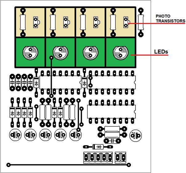
Fig. 4 – Mechanical construction of the sample circuit
Sample circuit experienceAs stated above, the sample circuit has been built and tested. Unfortunately it became clear that the output power of the IC1 is not high enough to drive the LEDs properly. Their light flux is too weak to drive the phototransistors properly and the circuit is capable of correct operation only when the LEDs are placed closer to the transistors. Anyway, the experiment has proven the philosophy of design and construction of the sample circuit is correct and with minor improvements the buttonless keyboard would be capable of the proper operation.
The reaction time of the sample circuit is lower than 200 µs and the output pulse length in case the button is hit is approximately 500 ms.
Future researchOn the basis of the positive experience with the presented construction philosophy, despite the partial failure of the sample circuit, the author decided to continue on constructing a 4x4 keyboard capable of cooperation with any microcontroller application considering the ideas stated below:
The layout of the keyboard that is intended to be constructed according to the above mentioned ideas is depicted in Fig. 5. The numbered fields represent the appropriate push buttons. Their numbers correspond to the order in which the LEDs are turned on. The red squares represent the photo sensors.
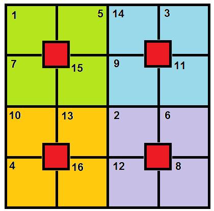
Fig. 5 – Example of 4x4 keyboard layout
ConclusionIn this paper a concept of the buttonless keyboard is described as well as the results gained in the experience with the sample circuit. Based on this experience the author worked out a proposal on the realisation of the 4x4 button board.
This paper is supported by the Internal Grant Agency at TBU in Zlin, project No. IGA/FAI/2012/056 and by the European Regional Development Fund under the project CEBIA-Tech No. CZ.1.05/2.1.00/03.0089.
References:[1] Trams, M., A Novel Concept for an Optical Push Button, Digital Force, 2007
[2] LEONI AG: Gebrauchsmusterschrift ”Optischer Schalter oder Taster”. Deutsches Patent– und Markenamt, Patent Number DE 20 2004 007 092 U1, October 20th 2005. See also http://publikationen.dpma.de
[3] Kingbright Web Site: http://www.us.kingbright.com
Aktuální číslo
Odborný vědecký časopis Trilobit | © 2009 - 2026 Fakulta aplikované informatiky UTB ve Zlíně | ISSN 1804-1795